
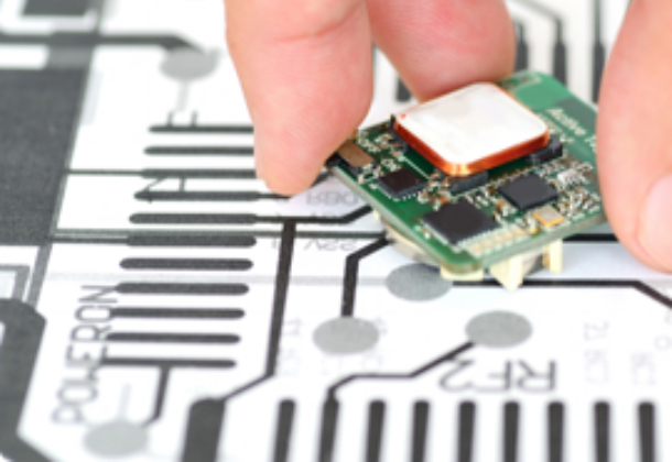
Printed Circuit Board Design
At Harlow Online Services we have over 30 years experience working with Printed Circuit Board (PCB) designs. What ever stage your ‘design’ is at we can take it and turn it into a professional printed circuit board.
Whether your ‘design’ is a functional sketch, electronic circuit or just an idea we can turn this into a functional printed circuit board. Using our Assembly Service we can assemble and test your circuit board for you too if this is required.
Supported Design Tools
Our supported tools currently are –
- Proteus Professional Design Suite
- BoardMaker 3 from Tsien (can also work with BoardMaker 2 PCB Designs)
- KiCad
- Altium Designer (limited)
If you have a requirement to develop using other tools please contact us and we will be happy to assist.
Circuit Diagram
A typical Project design cycle will start off with a clients sketch or idea. We will take this and turn it into a professional circuit diagram showing all the electronic components and how they are interconnected.
Once the circuit diagram has been completed this will be sent to the client for their approval.
Any required changes to the circuit can easily be made at this stage.

Printed Circuit Design
Once the client is happy with the circuit diagram the parts and interconnections are exported to the PCB layout tool.
We then proceed to lay up the printed circuit board (PCB). This will usually start with a PCB foot print to fit within the clients requirements and then placement of critical parts and fixings followed by all the other components.
Once the components are placed we will the proceed to route the PCB according to the clients required design rules. When the PCB is fully routed and all design rule checks are completed this is sent to the client for approval.
Any required changes are then made to the layout until the client is able to approve the PCB design.

Data Processing
The data processing then takes place generating all of the data that the client requires for their project. All of this data is then packaged into the Client Release Pack for the Project. This is then delivered to the client.
Each clients post design requirements are unique but we will work with you to ensure that you receive all the data that you require. As a minimum this will be the final PCB Design file (for whatever design tools you select). As well as this basic information we can provide RS274X Gerber and Excellon drill data, pick and place outputs, parts lists and build instructions. Exports can be in PDF, IDF, DXF or BMP.

Standards and Design Rules
All of the way through the design process we ensure that we are working to ensure that all traces on the Printed Circuit Board are the correct thickness for the required current capacity and spacings are suitable for reliable operation based on the clients preferred specification whether the design is required to UL 60950-1, IPC-2221 or IPC9592 standards. Typically our designs are undertaken to IPC-2221B but if the client requires and alternative then we are happy to work within these.
When the PCB design is completed it is checked against the net list and the defined design rules to ensure that all is as it should be.

PCB Specification
Our PCB design work can consist of both surface mount and through hole parts with surface mounted parts on the top side, bottom side or both top and bottom sides.
Our PCBs can have between 1 and 32 tracking layers (most of our boards are double sided or 4 layers) and can be up to 40 inches square!.
Any logos can be added to either of the silk screen layers or tracking layers if required.
All of our boards are designed to be economical to produce within the standard manufacturing specification of most PCB manufacturers.
All design work is carried out within the scope of our ISO 9001:2015 certification.